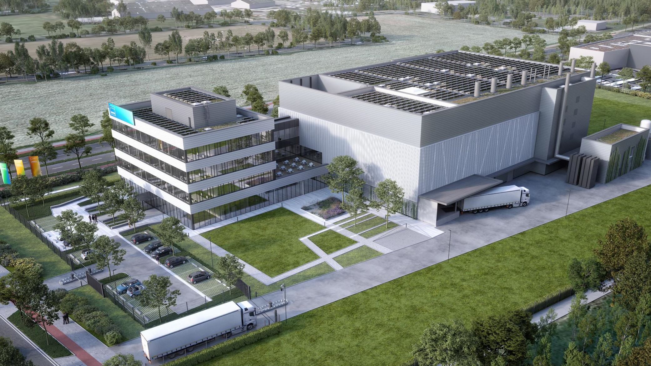
More high-tech in Silicon Saxony: The Jenoptik fab in Dresden
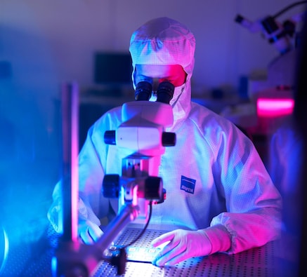
After around two and a half years of construction, the Jenoptik Group has completed its largest single investment in recent history and officially inaugurated its new fab in Dresden, Germany for the manufacture micro-optics and sensors for the semiconductor equipment industry. Discover more about this investment in a high-tech manufacturing facility.

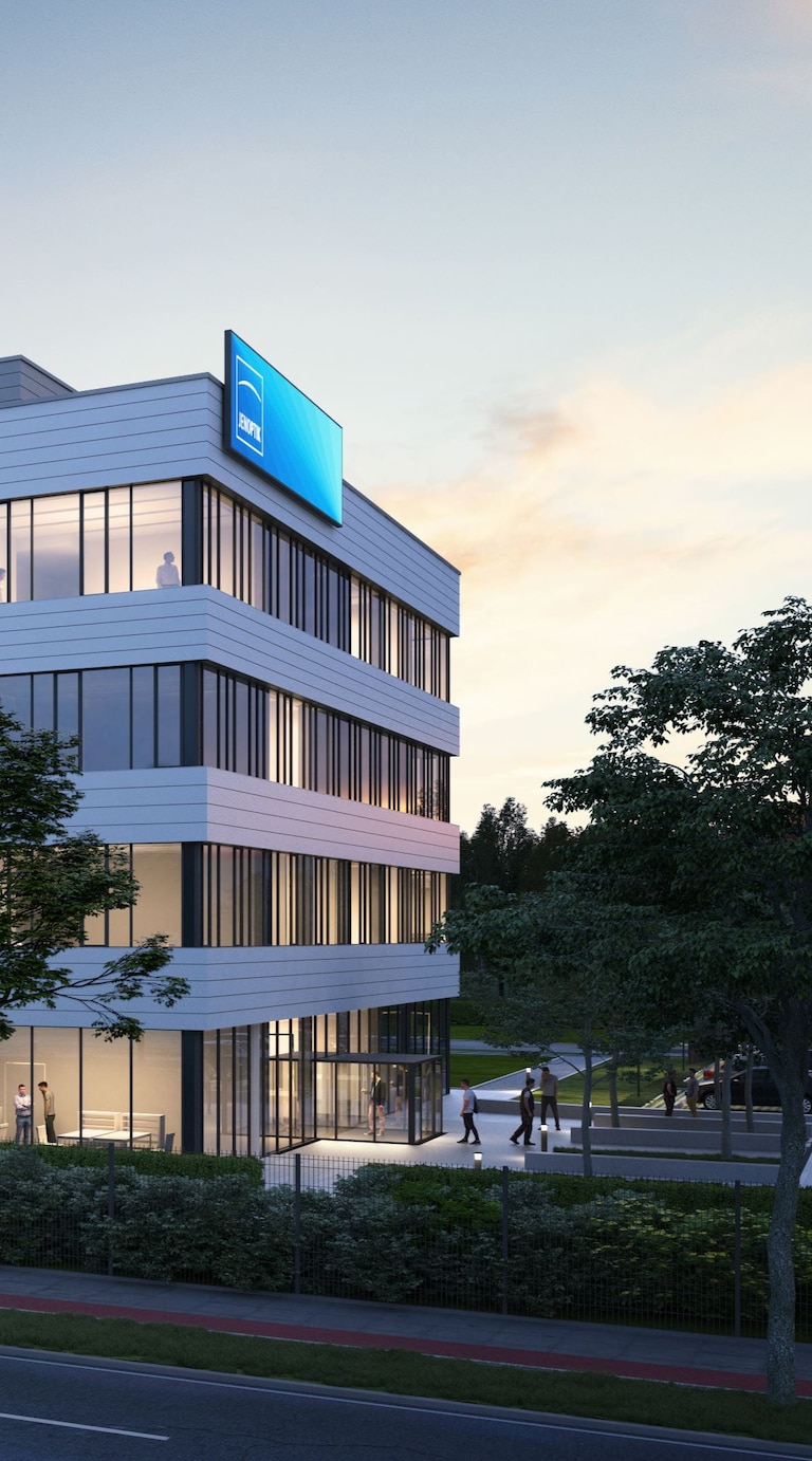
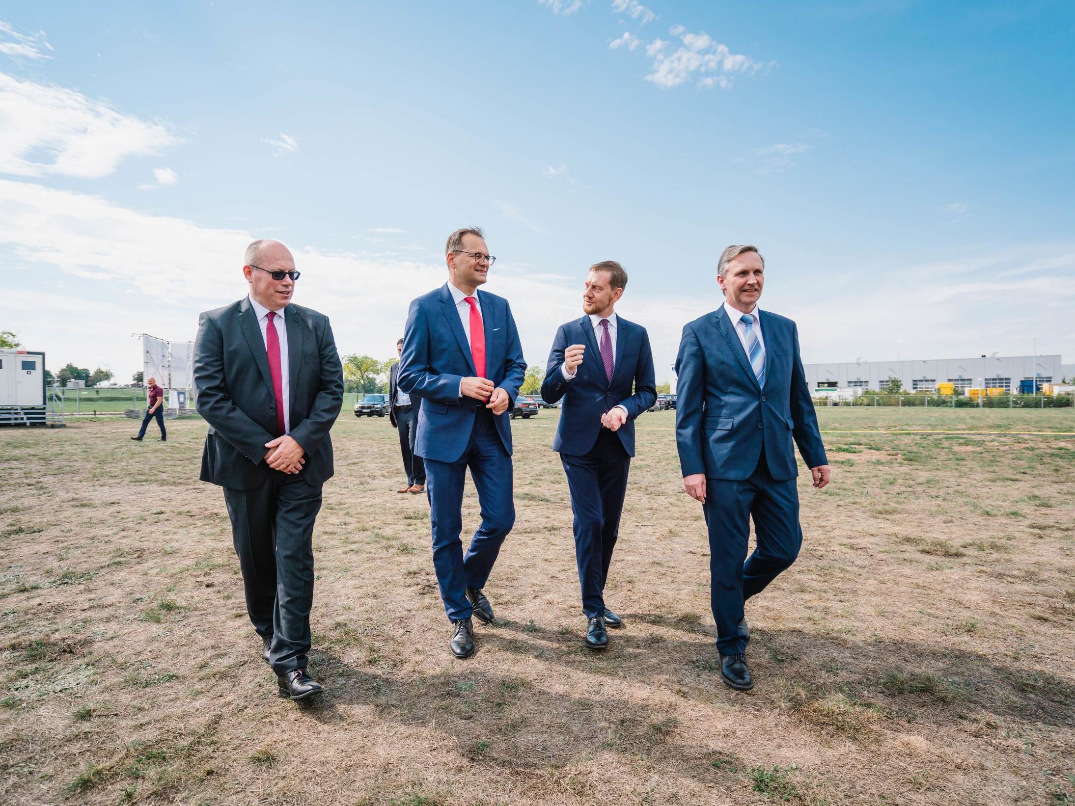
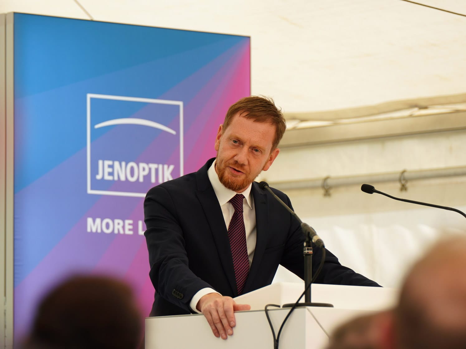
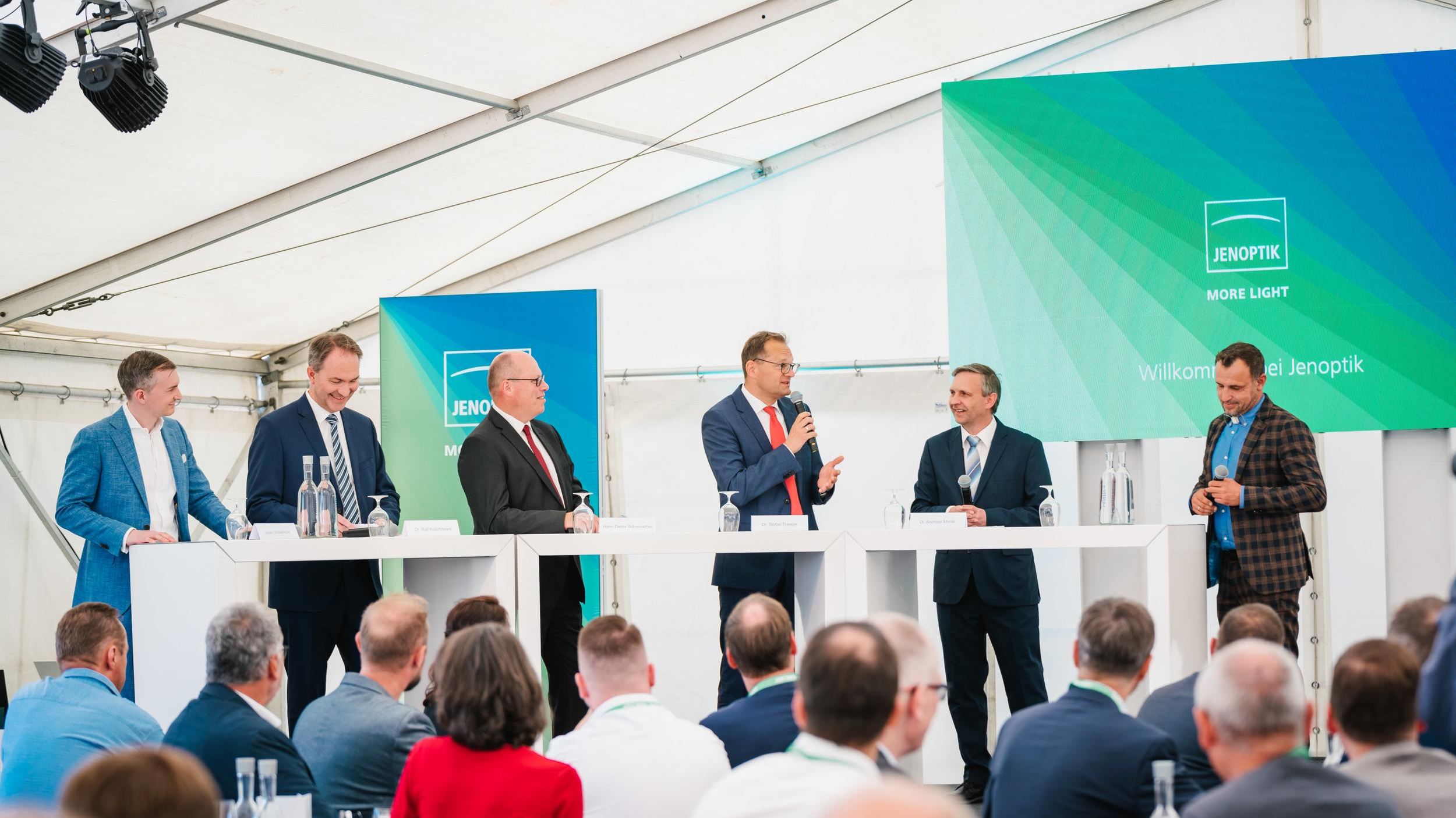
The new Jenoptik fab in Dresden was officially opened on May 6, 2025 in the presence of customers, partners, construction stakeholders, neighbors, and representatives from business, politics, and government agencies of the Free State of Saxony and the City of Dresden. Together with the Minister President of the Free State of Saxony, Michael Kretschmer, and the Lord Mayor of the City of Dresden, Dirk Hilbert, Jenoptik President & CEO Dr. Stefan Traeger and Site Manager Dr. Andreas Morak opened the fab in Dresden, in the heart of the semiconductor hub called 'Silicon Saxony'.
Previously, exactly one year after the groundbreaking ceremony on September 6, 2022, Jenoptik celebrated the topping-out ceremony for its new high-tech factory on September 6, 2023.
©studiobrand.3dvisuals
Our new factory will be ready for manufacturing in 2025. We're confident to start operation as scheduled and invite you to become part of our Jenoptik team in Dresden today!
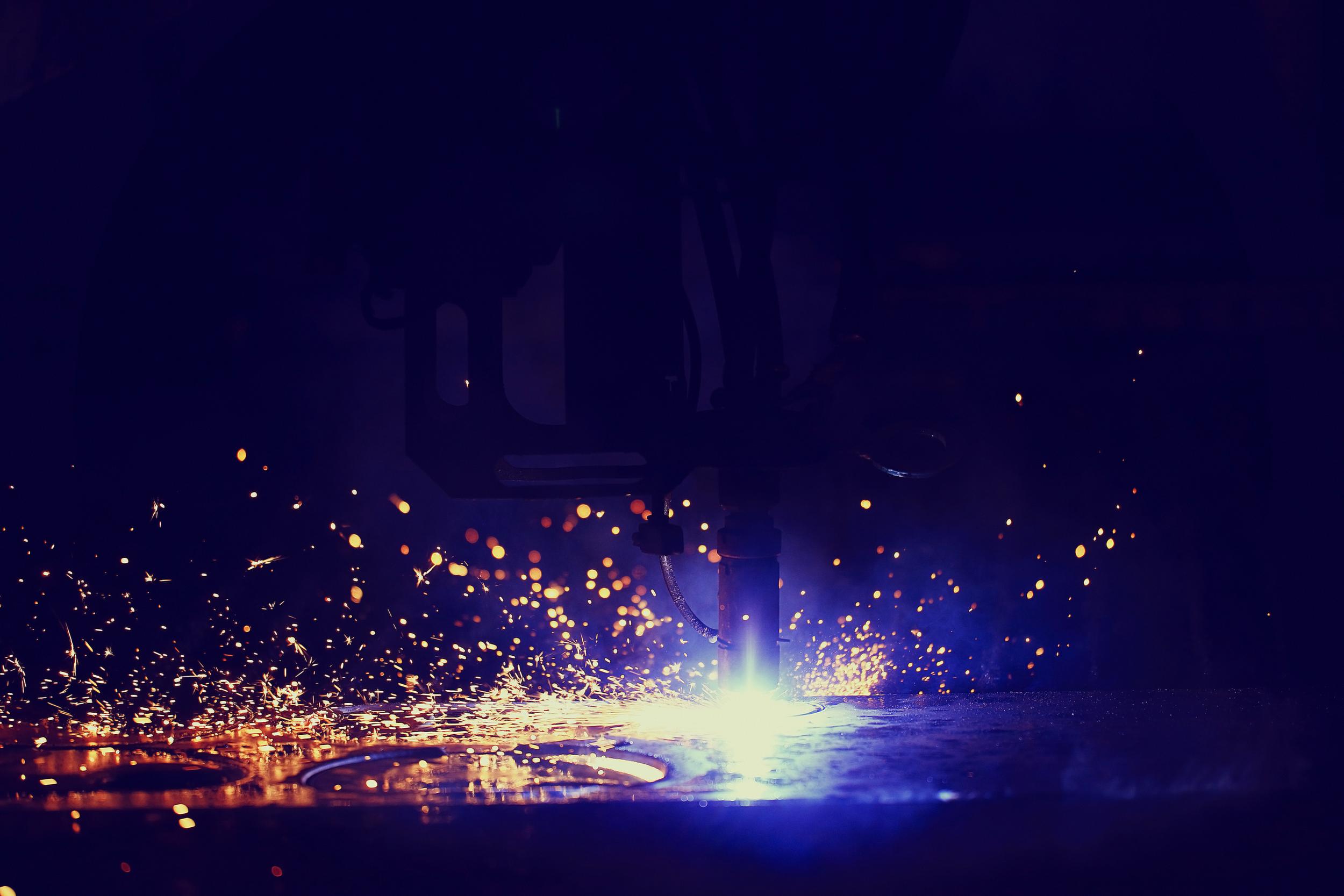
Extremely demanding construction and manufacturing environment
High environmental standards taken into account

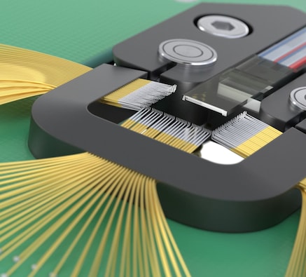
Dresden as a major micro-optics location
Photonics as a growth driver
These were the milestones on the construction site
Take a closer look at the future high-tech factory in the video!
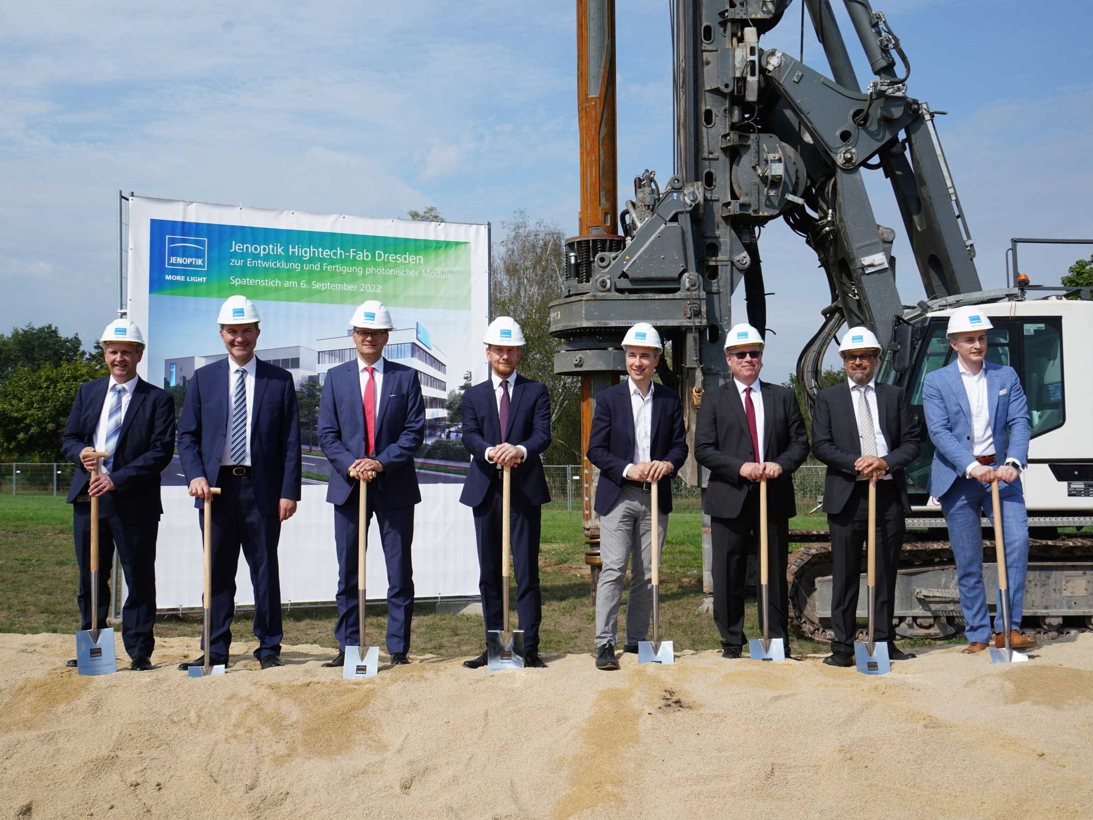
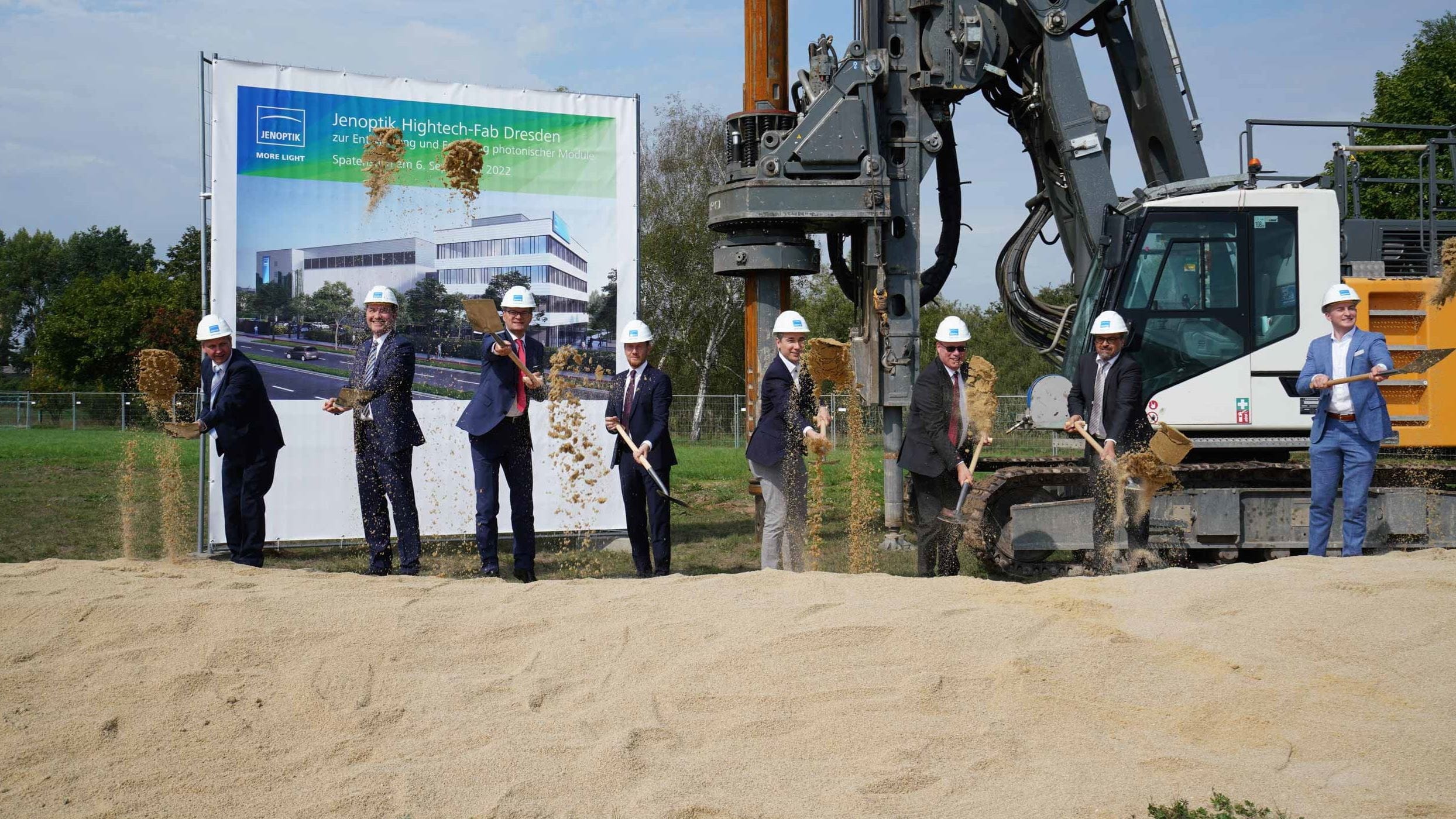
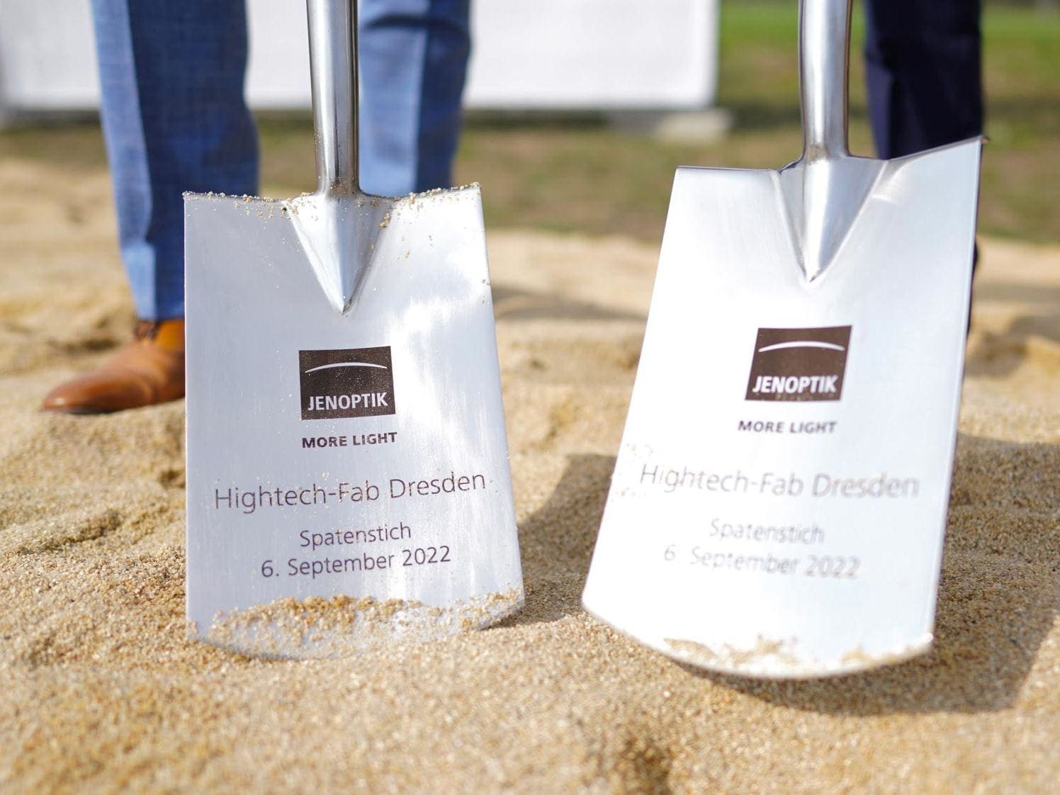
Images from the groundbreaking ceremony (©Benjamin Jehne)
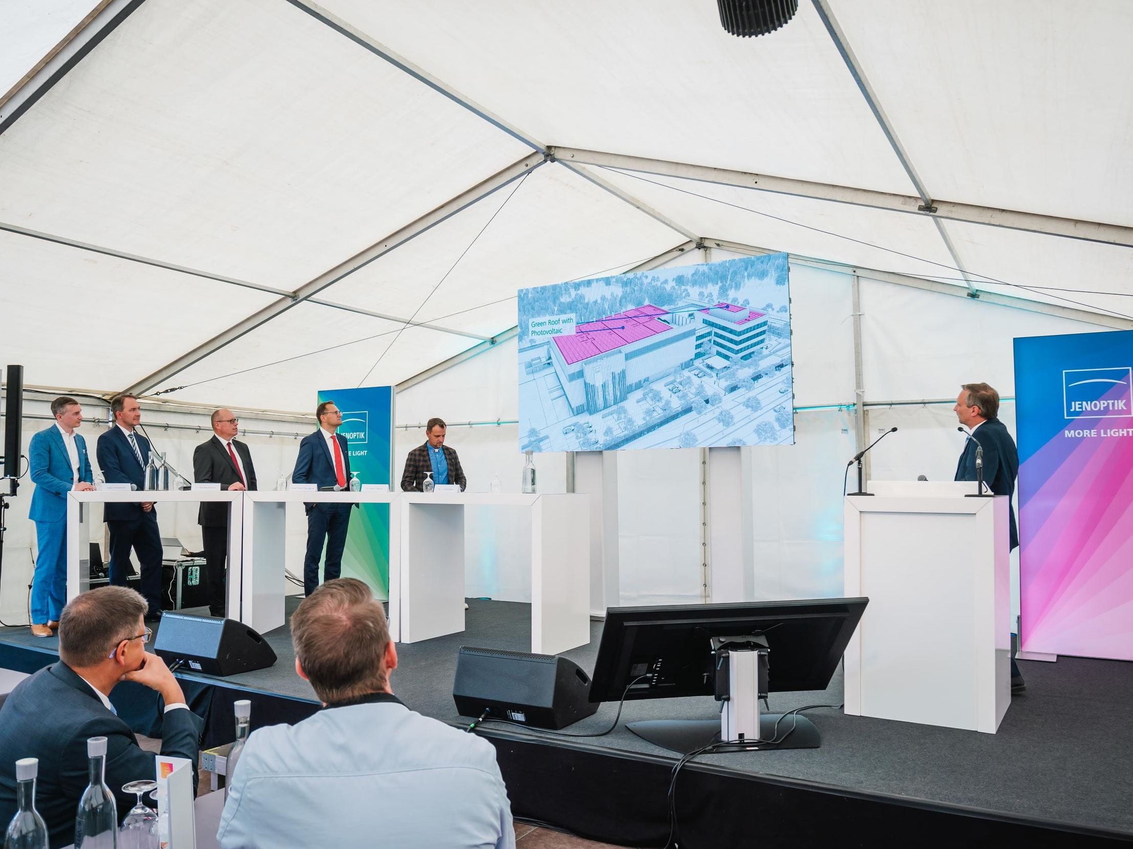
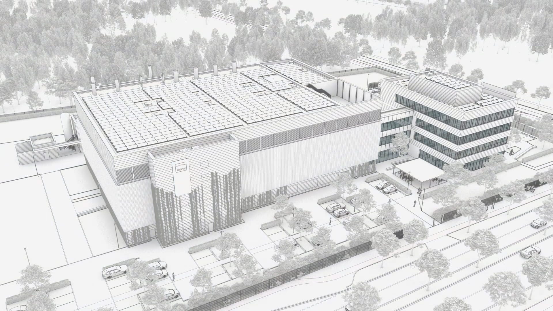
Total net area: approximately 11,000 sqm, with space for ...
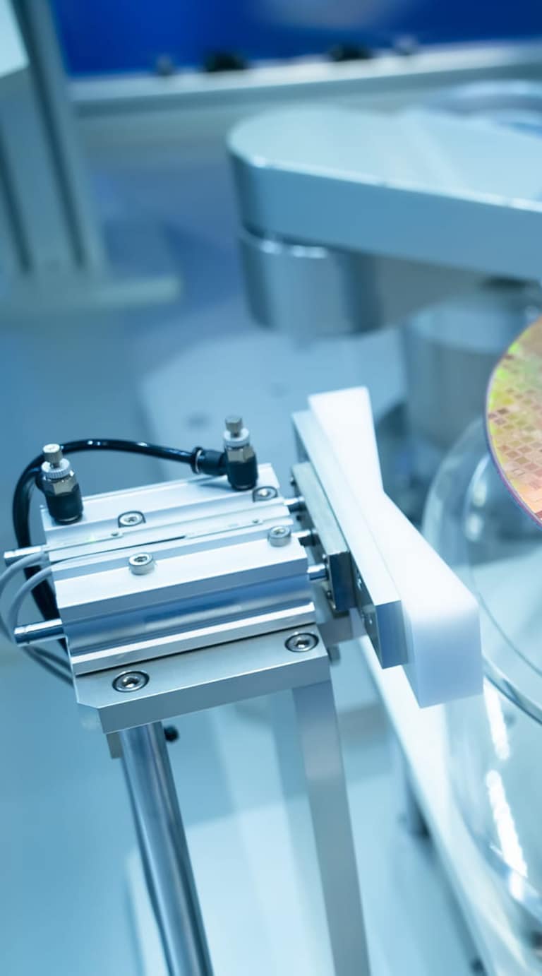
clean room/ production
logistics
technical areas
offices & admin
showroom, meeting & reception areas