RecommendMail Facebook LinkedIn
UFO Probe® card – new test card for PIC wafer testing
Photonic Integrated Circuits (PICs) are the chips of the future. Integrated photonics use light instead of electricity for data and signal processing.
Speed up the world

UFO Probe® Technology keeps you one step ahead
Built-in solution for high-volume production

New Jenoptik UFO Probe® Vertical

As the Cantilever Version, the UFO Probe® Vertical enables parallel functional tests of optical as well as electrical components on chips using vertical needle technology from MPI. This allows the user to couple up to 32 optical channels in parallel as standard - or more if required - without the need for active alignment.
Opto-electronics tests with high throughputs:
- Covers wavelength range from 1260 to 1625 nm used in the telecom and datacom sector
- Ability to provide polarization maintaining for individual or all optical channels
- Testing of bond pads, solder bumps or copper pillars
- Contacts up to tens of thousands of bond pads with dimensions down to 35µm.
- Smallest addressable pitch of electrical contacts from 40 to 80 µm
- Vertical probes with lower and more uniform contact resistance from 0.2 to 1.0 ohms, depending on the probe type, while minimizing probe marks.
- Ensure economical use in high-volume test scenarios and ATE operability.
All benefits of the Probe Card Technology on one view
Progress
The PIC ecosystem can be expanded thanks to an efficient test method for high-throughput serial production; and the test time is reduced thanks to parallel qualification of multiple chips.
Innovation
The only commercial test solution for high-volume production that can run on standard test equipment.
Quality
Scrap is identified at an early stage of production for improved yield: All testing of all PICs can be carried out on a wafer.
Plug and Play
It is designed to operate in standard IC testers and automated testers. Low outlay and commissioning costs.
Efficiency
Fault parts are identified early on for increased yield and optimized production flow.
Flexibility
The pitch and number of optical I/O channels can be configured to suit you.
Enabling optical data communication

Probe card applications now and in the future


They can easily be integrated into existing test infrastructure
The UFO Probe® card is intended for operation on standard IC probers and/or automated test equipment. So, Jenoptik offers a plug-and-play solution for PIC wafer level tests. Depending on requirements, standard interfaces to wafer samplers can be easily implemented in the layout/design of the probe card – for example, in European card format. UFO Probe® card is used like electrical test cards, so current personnel won't need extensive extra training.


Combination of novel optical concept and proven needle technology
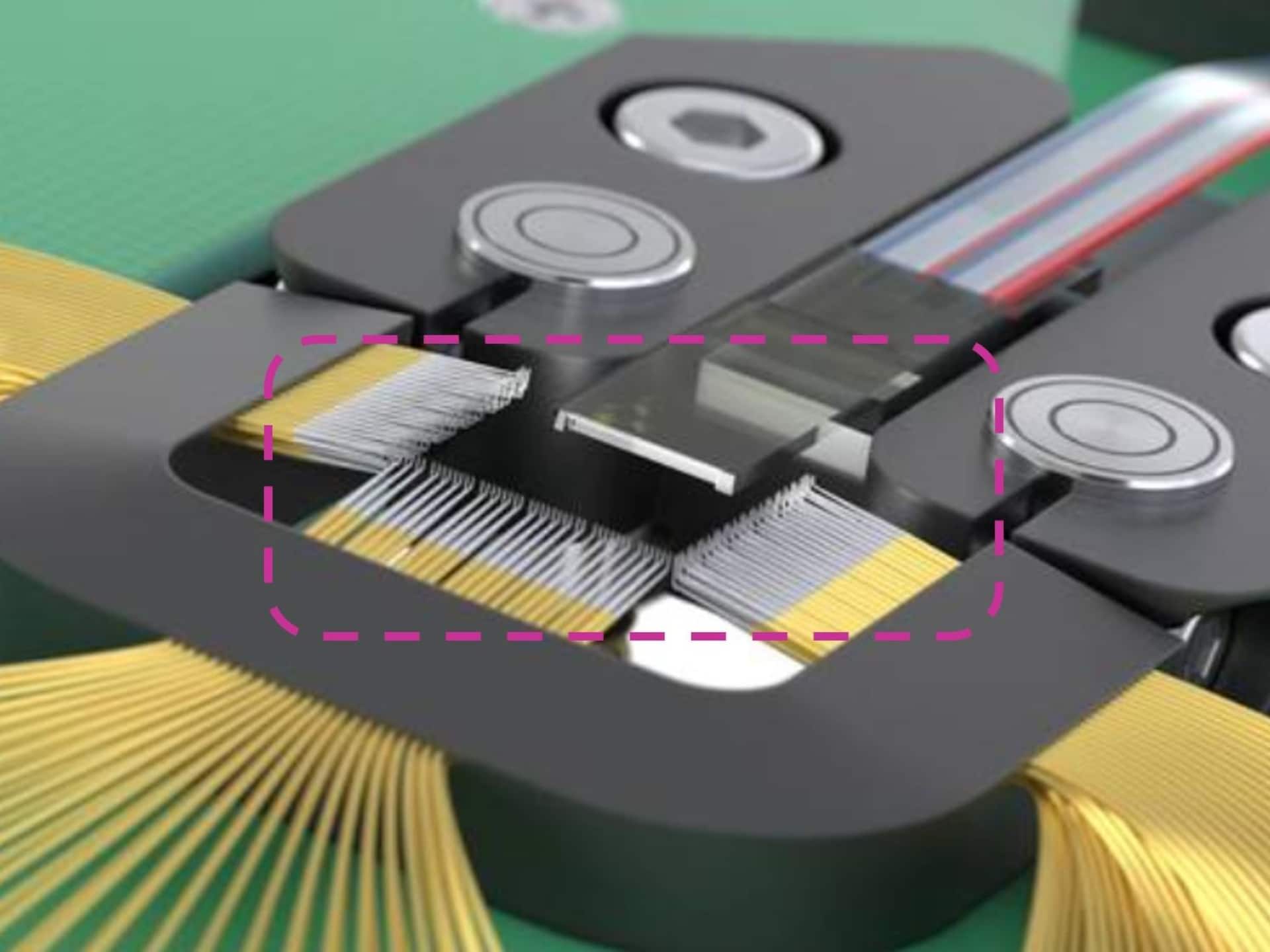

- Monolithic optical module
- Alignment-insensitive optical coupling for vertically emitting PICs
- Simultaneous optical and electrical contacting
- Optical concept compensates prober alignment tolerances
- Use of proven needle technology (partnership with test card manufacturers)
- Standard interface to wafer prober
Technical details of the UFO Probe® optoelectronic card
| Specifications | Current generation | Future generations |
|---|---|---|
Component to be tested | Electronic and photonic integrated circuit (EPIC); optical transceivers for data transmission and telecommunications applications | EPIC for transceivers, photodiodes, |
Electric needle technology | Cantilever and Vertical | Cantilever, vertical/advanced |
Optical coupling principle DUT | Vertical coupling | Vertical coupling |
Number of optical inputs/outputs (OI/OO) | Up to 32 or more | <200 |
Pitch OI/OO | 127 μm, 250 μm, flexible for >250 μm | flexible |
Layout configuration of OI/OO arrays | Linear arrangement with same direction of inputs/outputs | Configurable to own needs |
Coupling angle | 0° and 11.6° standard, up to 20° customized | 0° - 20° |
Supported wavelength | 1260 - 1625 nm (O/ L-band) | VIS to NIR (U-band) |
Measurement of insertion loss | Repeatability: ~ 0.3 – 0.5 dB | Repeatability target: 0.1 dB |
RF measurement | Up to 110 GHz, depending on needle technology | GHz |
Interfaces | Eurocard format; ATE* | Eurocard format; |
Customized for your success
Based on the UFO Probe Technology, we will customize a specific opto-electronic test solution that will fit the complex demands of your application.
Each UFO Probe® Card is customized to the individual requirements and the respective wafer layout and is available with both cantilever and vertical needle technology. Check out the specifications for more details.

Your partner in PIC testing
Jenoptik has profound expertise and know-how in micro-optics and optics and we are a competent and valuable partner to the semiconductor industry for many years. We know and understand the challenges of our customers and combine these with our technical experience and knowledge to create innovative solutions, such as the UFO Probe®Card. The necessary skills and the continuous development of technologies is just one aspect that we pursue with one goal: Moving you forward.
High-Performance from A to Z – our competencies:
- Design: Optical module and general electrical and optical probe card card
- Manufacturing and supply chain management
- Micro-assembly and alignment of optical and electrical modules
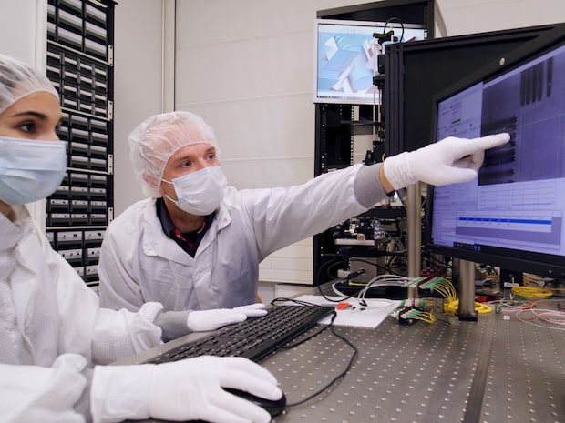
- Optical test and verification in lab: customized test rig
- Test under manufacturing conditions: Accretech UF3000 Prober
Have a closer look to the UFO Probe® Vertical

Do you have any questions? Our experts will be happy to help you!
Awarded! Thuringia Innovation Award 2022 for UFO Probe® card
Jenoptik was awarded the Thuringia Innovation Award 2022 in the "Industry & Materials" category on November 30, 2022 in Weimar, Thuringia for its novel opto-electronic probe card for testing PIC wafers. Not quite 100 applications were received by STIFT Thüringen this year. Jenoptik convinced the expert jury with its well-thought-out approach to solving the increasing demand for photonic technologies in the electronics and semiconductor industry.